


Having spent time at Intel, navigating the massive complexities where semiconductors meets cloud-native software, you develop a certain idea of scale. You get used to big numbers and complex systems. But every now and then, you encounter a piece of engineering so audaciously complex that it resets your baseline for what is possible.
The B1M recently released a fantastic mini-documentary on ASML’s Extreme Ultraviolet (EUV) lithography machine. Even for those of us who have lived inside the semiconductor ecosystem, the sheer complexity and precision required to manufacture modern chips is mind-bending.
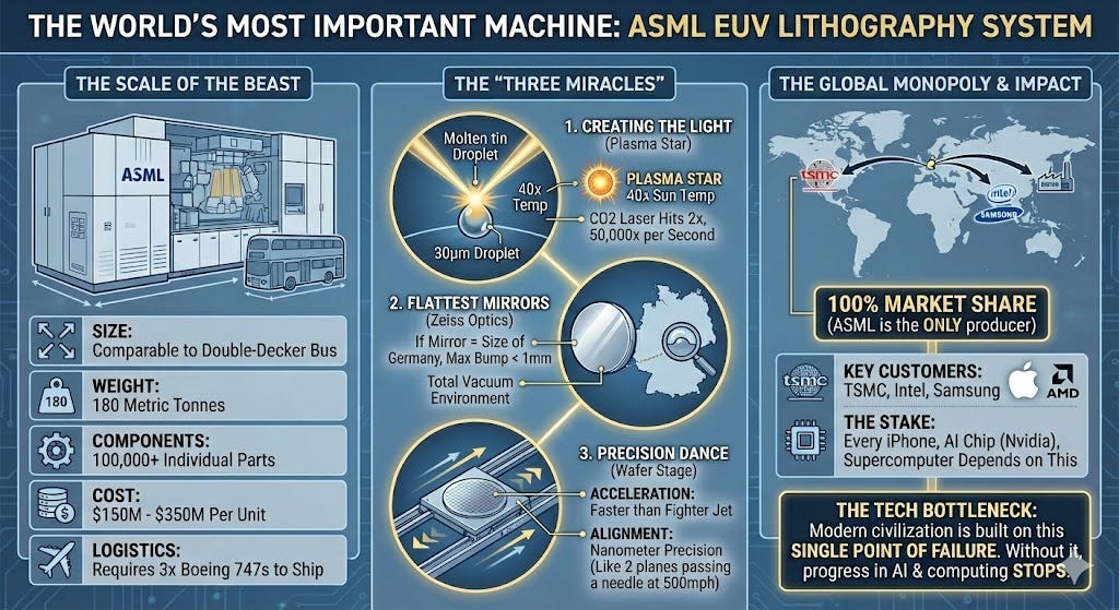
The video captures the reality that Moore’s Law isn’t continuing because of simple evolution; it’s continuing because of brute-force physics and “ridiculous engineering.” We had hit a wall where traditional lightwaves are too large to print the nanometer-scale features required for today’s AI and mobile processors.
The solution, as detailed in the documentary, involves what are essentially three concurrent engineering “miracles.”
To generate the specific 13.5nm wavelength of light needed, the machine doesn’t just turn on a lamp. It drops a microscopic globule of molten tin and hits it mid-fall with a high-powered CO2 laser—three times. The first hit flattens it, the second does rarefaction, the third vaporizes it into plasma that is 40 times hotter than the surface of the sun. The machine does this 50,000 times every single second to produce the high energy wavelength of light needed to etch the transistors.
Because this EUV light is absorbed by almost everything, including air and glass, the entire process must happen in a high-vacuum environment using mirrors rather than lenses. These aren’t normal mirrors; they are crafted by Zeiss to be the flattest surfaces ever made. The video uses a great analogy: if one of these mirrors were scaled to the size of Germany, the highest mountain on it would be less than a millimeter tall.
Simultaneously, the stage holding the silicon wafer is accelerating faster than a fighter jet, yet it must align itself with nanometer precision to catch that light pattern.
It is a stunning ballet of plasma physics and hyper-precision optics happening inside a box the size of a double-decker bus.
A Terrifyingly Fragile Foundation
The engineering is fascinating, but the business implications are sobering. As the video concludes, and I became acutely aware of during my time at Intel, this machine is perhaps the most critical single point of failure in the modern economy. And contributes to various geopolitical flashpoints still developing.
ASML has a 100% market share for EUV. There is no alternative. Every top-tier chip manufacturer—from TSMC to my former colleagues at Intel—relies entirely on this one company in the Netherlands to produce the silicon that powers everything from iPhones to NVIDIA’s AI infrastructure.
It is a geopolitical moat, an engineering marvel, and a terrifying supply chain bottleneck all wrapped into one $350 million device. It serves as a potent reminder that underneath the abstract layers of software and SaaS business models, the digital world rests on a physical foundation of truly “impossible” engineering.